Configurable, extensible processor cores run Linux
Dec 4, 2006 — by LinuxDevices Staff — from the LinuxDevices Archive — 12 views[Updated Nov. 3, 2008] — Tensilica is shipping two new processor core families based on its “post-RISC” style Xtensa architecture. The LX2 and Xtensa 7 cores are available with MontaVista Linux, and come with tools aimed at helping designers configure interfaces, memory subsystems, and other components, and even extend the architecture with C/C++ application-specific instructions.
Both processors are based on the seventh generation of Tensilica's Xtensa architecture. The company claims that customers can use the cores and associated tools to create custom SoCs (system-on-chip processors) with unrivaled performance and power characteristics.
The Xtensa 7 targets low-power applications, such as embedded control and digital signal processing. In its most basic configuration, it compares to ARM's ARM7TDMI-s cores, albeit with more performance and lower power, Tensilica says.
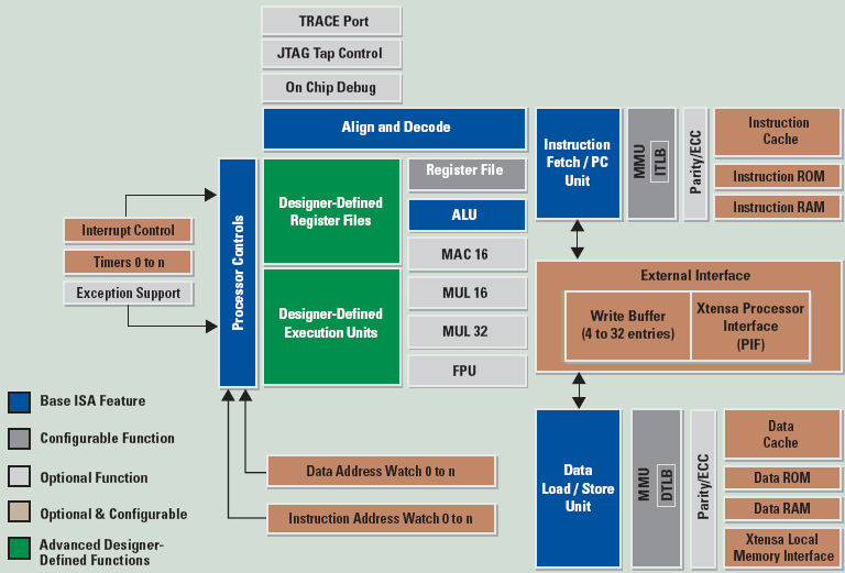
Tensilica Xtensa 7 functional diagram
(Click to enlarge)
Tensilica claims that a 233-250MHz Xtensa 7 core delivers 300 DMIPS (Dhrystone millions of instructions per second) while drawing a mere 0.082mW per MHz. Meanwhile, an ARM7TDMI-S clocked at 146MHz delivers only 131 DMIPS, while drawing between 0.10 and 0.18mW per clock cycle, according to the company.
The Xtensa LX2 incorporates additional capabilities apparently aimed at competing with ARM9 and ARM11 cores, including:
- Faster I/O
- Optional multiple instructions per cycle “in a manner similar to VLIW processors”
- Optional 7-stage pipeline clockable to 650 MHz in 90nm GT process
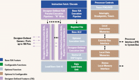
Tensilica Xtensa LX2 architecture diagram
(Click to enlarge)
Tensilica claims a performance-optimized general-purpose LX2 core occupies half the die area of an ARM 1136J-S, delivers five times more performance in EEMBC benchmarks, and draws 0.17 versus 0.60mW per MHz, when built on .13-micron process technology.
Common to both cores is a new on-the-fly ECC (error correction code) option, important for storage, networking, safety-critical automotive applications, according to Tensilica.
Also new are a bevy of power-sparing options, including:
- Independent width selection of main system memory interface, local data memory interface, and instruction memory interface
- Reduced execution speculation for data memory enables and accesses, leaving data cache and tightly coupled local data memories turned off for longer periods of time
- An optional wider instruction fetch buffer that reduces instruction memory cycles
- Power-down modes for trace port and on-chip debug modules
Tensilica claims that cumulatively, these features can result in 30 percent lower power requirements than processors based on its earlier Xtensa 6 architecture, released about a year ago.
Overall, Tensilica says its configurable Xtensa processors outperform dedicated hard-wired RTL (register-transfer level) IP blocks in several ways, including: flexibility; the ability to implement bug fixes via firmware; shorter design and verification time; and lower power consumption.
Availability
Both the Xtensa 7 and Xtensa LX2 processors are shipping now. Xtensa 7 pricing starts at $250,000 for a single-project use license. Linux is available from Tensilica partner MontaVista.
This article was originally published on LinuxDevices.com and has been donated to the open source community by QuinStreet Inc. Please visit LinuxToday.com for up-to-date news and articles about Linux and open source.