IBM plots path to denser chips
Feb 20, 2006 — by LinuxDevices Staff — from the LinuxDevices Archive — views IBM researchers say they have found a way to shrink microprocessors and other silicon chips by more than two thirds without requiring fundamentally more expensive process technologies. The company claims it has created “the smallest, high-quality line patterns ever made,” with features measuring 29.9 nanometers, using a… variant of standard DUV (deep ultraviolet) chip printing methods.
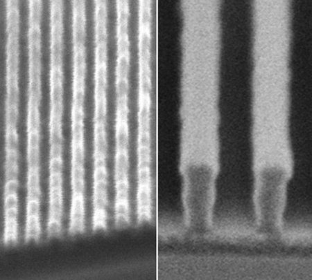
The research group said the appoach can yield “distinct and uniformly spaced ridges” that are 29.9 nanometers wide, which offers a way to make chips with more than three times the density of today's production chips that have recently attained 90-nanometer features. Additionally, IBM said the technique breaks the 32 nanometer barrier thought to have been limiting the density of chips made with optical lithography chip-printing processes.
IBM's new 29.9 nm line widths vs. today's typical 90 nm widths
(Source: IBM Research)
For the past 40 years, Intel and other semiconductor manufacturing companies have been able to produce chips with continually increasing density — and hence performance — adhering to a principle popularly known as “Moore's law”.
Simply stated, Moore's law, articulated in 1965 by Intel co-founder Gordon Moore, states that chip transistor densities tend to double every two years.
“But as chip features now approach the fundamental scale limits of individual atoms and molecules, the future of this trend of relentless improvement, known as Moore's Law, is being threatened,” according to IBM.
In its announcement Monday, IBM said that its latest accomplishment, described as a “high-index immersion variant of DUV lithography,” offers the opportunity of extending Moore's law and “buying the industry time” before a “high-risk conversion to an extremely expensive alternative” is required.
“Our goal is to push optical lithography as far as we can so the industry does not have to move to any expensive alternatives until absolutely necessary,” said Dr. Robert D. Allen, manager of lithography materials at IBM's Almaden Research Center. “This result is the strongest evidence to date that the industry may have at least seven years of breathing room before any radical changes in chip-making techniques would be needed.”
Technical details of IBM's chip printing breakthrough will be disclosed Monday at the SPIE Microlithography 2006 conference in San Jose, Calif., IBM said.
This article was originally published on LinuxDevices.com and has been donated to the open source community by QuinStreet Inc. Please visit LinuxToday.com for up-to-date news and articles about Linux and open source.