Intel touts phase-change memory breakthrough
Oct 28, 2009 — by LinuxDevices Staff — from the LinuxDevices Archive — 4 viewsIntel and Numonyx announced a “key breakthrough” in the development of phase change memory (PCM). For the first time, researchers have created a 64Mb test chip demonstrating the ability to stack multiple PCM arrays within a single die, the companies said.
Unlike DRAM or flash memory, PCM uses heat to store data, not electrons. The technology uses chalcogenide glass, which contains elements such as sulphur, selenium, or tellurium. This material, which has also been used on rewritable optical media, can exist in both crystalline and amorphous states. Heat is used to toggle between them, thereby storing a single bit of information.
PCM's advocates — which have included Samsung as well as Intel and Numonyx — note that flash memory stores data by modulating electrons stored within the gate of a transistor, requiring relatively large voltages and amounts of time. It's said that PCM can offer substantially lower power consumption, and speed approaching that of DRAM.
Another cited advantage of PCM is bit alterability, meaning that a single bit can be changed at any time. With flash, changing one bit can require erasing a "block" of data that may contain hundreds or even thousands of bits. This slows down writes and increases wear.
A new breakthrough
Intel and Numonyx say their researchers have now found a way to stack multiple PCM arrays within a single die, increasing memory density. The new technology is called PCMS (phase change memory and switch), and combines a PCM element with a thin-film selector called an Ovonic Threshold Switch (OTS).
Thanks to the presence of the OTS selectors, it will be possible to layer multiple PCM elements together on a single CMOS base, creating high-density, high-bandwidth PCM memory, the companies promise. However, today's announcement was of a 64Mb PCMS test chip that includes only a single PCM element.
An article for the Channel Register website quotes Al Fazio, Intel fellow and director of memory technology development, as saying that PCMS will allow PCM to break through NAND flash memory's 20nm barrier, scaling down to process sizes as tiny as 5nm. However, both Fazio and Greg Atwood, a senior technology fellow at Numonyx, are said to have conceded that a commercial product based on PCMS is still years away.
Fazio said in a statement, "We continue to develop the technology pipeline for memories in order to advance the computing platform. We are encouraged by this research milestone and see future memory technologies, such as PCMS, as critical for extending the role of memory in computing solutions and in expanding the capabilities for performance and memory scaling."
Atwood stated, "The results show the potential for higher density, scalable arrays and NAND-like usage models for PCM products in the future. This is important as traditional flash memory technologies face certain physical limits and reliability issues, yet demand for memory continues to rise in everything from mobile phones to data centers."
Background
Intel has been working on PCM technology since the early part of this decade, and continues to develop it in conjunction with Numonyx, an independent semiconductor company it spun off last year as a joint venture with STMicroelectronics and investment company Francisco Partners. Last year, Numonyx began sampling a 128MB, 90nm PCM implementation code-named "Alverstone."
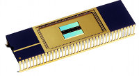 Meanwhile, another key advocate of PCM is Samsung, which prefers to describe the technology as PRAM (phase change random access memory). Samsung has been working on PRAM since at least 2006, when it unveiled the first working prototype (right) of a 512Mb component.
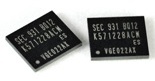 In September, Samsung announced that it is producing 512Mb (64MB) PRAMs (left) using 60nm technology. The company's PRAM is claimed to be more than ten times faster than NOR flash, erasing 64 Kilowords (KW) in 80ms. In data segments of 5MB, PRAM can erase and rewrite data approximately seven times faster, Samsung adds.
Citing "greatly simplified data access logic that requires less support from DRAM," Samsung said PRAM makes very efficient use of power. Handsets that use PRAM will be able to offer 20 percent better battery life, the company added.
Further information
Intel and Numonyx said they will publish more information about PCMS memory in a paper, "A Stackable Cross Point Phase Change Memory," that will be presented at the 2009 International Electron Devices Meeting in Baltimore on Dec. 9. Co-authored by Intel and Numonyx technologists, the paper will be presented by DerChang Kau, Intel senior principal engineer, according to the companies.
To read the Channel Register article alluded to above, see the publication's website, here.
This article was originally published on LinuxDevices.com and has been donated to the open source community by QuinStreet Inc. Please visit LinuxToday.com for up-to-date news and articles about Linux and open source.