Samsung bakes 8 gigabit NAND flash chips
Jul 20, 2006 — by LinuxDevices Staff — from the LinuxDevices Archive — 2 views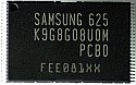 NAND flash chipmaker Samsung Electronics says it has entered into mass production of an 8 gigabit NAND flash memory chip aimed at mobile phones, MP3 players, gaming consoles, and other consumer devices. The high-density MLC (multi-level-cell) memory is fabbed in 60 nanometer process technology, “the smallest used today,” according to the company.
The arrival of the chip coincides with what Samsung calls the “New Memory Growth Model” — double density growth every 12 months. The growth pattern, reminiscent of Moore's Law, was conceived by Dr. Chang Gyu Hwang, CEO of Samsung Electronics Semiconductor Business, Samsung says. Simply stated, Moore's law, articulated in 1965 by Intel co-founder Gordon Moore, states that chip transistor densities tend to double every two years.
Samsung will incorporate the new 8Gb chip in an 8 gigabyte (GB) device containing 4GB packages, each carrying a vertical stack of four 8Gb dies, the company said. The 8GB NAND device is expected to reach production in the third quarter of 2006.
The 8Gb chip will also be incorporated into several other Samsung high-density NAND solutions, targeting mobile handsets among other mobile and embedded applications.
According to Samsung, the new 60nm fabrication technology offers 25 percent higher manufacturing capacity relative to the previous 70nm design technology, a factor that can be expected to result in lower-cost flash chips and memory cards.
This article was originally published on LinuxDevices.com and has been donated to the open source community by QuinStreet Inc. Please visit LinuxToday.com for up-to-date news and articles about Linux and open source.