Article: Moving toward NAND and NOR convergence
Aug 29, 2006 — by LinuxDevices Staff — from the LinuxDevices Archive — 3 viewsIntroduction
NAND and NOR technologies each have distinct advantages for developers and end customers, and there is a growing trend toward designing systems capable of converging these technologies. Many existing designs deploy both NAND and NOR arrays. New technologies such as Samsung OneNAND and Spansion OrNAND seek to offer the benefits of NAND and NOR within a single solution, while… integrated NAND controllers simplify system design.
This paper examines the advantages and disadvantages of these two flash technologies — NAND and NOR — and then looks at how these technologies are converging.
NAND vs. NOR cell organization
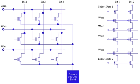
Following are illustrations of a typical NOR cell organization (left) compared to a typical NAND cell organization (right). NOR allows for individual access to each cell, whereas NAND accesses each cell through adjacent cells.

Differing cell designs: NOR (left), NAND (right)
(Click to enlarge)
NOR attributes
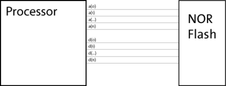
The advantages of NOR for the developer are realized by a few specific features. NOR provides a serial interface to an embedded system just like RAM, making it more developer friendly than NAND.

NOR ships with all blocks known as “good” and has high erase counts which make for long life in the field. NOR also allows for a code to execute directly from within an NOR chip, not requiring that code be copied to RAM to be executed. The result of this eXecute In Place (XIP) feature is that NOR can offer fast boot times by jumping directly to an operating system stored in NOR and boot. NOR has been a widely adapted, widely successful technology, used for fast read, low density environments and there have been very few innovations seen within NOR technologies over the last several years.
90nm Intel NOR — “Sibley”
One notable exception is the 90nm Intel NOR device code named “Sibley.” Sibley is targeted directly for the consumer mobile market segment, and is the first NOR multi-level cell (MLC) flash memory device manufactured on Intel's leading 90 nanometer technologies. The Sibley family offers fast NOR read speeds to enable zero-wait code execution at up to 108 MHz. In addition, Sibley writes speeds of up to 500 Kilobytes per second, enabling the rapid data storage of multimedia images required in today's wireless handsets. This product family will increase the NOR flash density reach with a monolithic 512Mb device, as well as support multiple RAM interfaces to provide the greatest design flexibility for cellular OEMs.
NAND attributes
NAND flash evolved from byte-addressable EEPROM with a design goal to have a low cost per bit selling point. NAND flash is available in high densities with fast write access making it ideal for data storage devices. However, there are certain complexities to using NAND flash in a system. First, unlike most processors its pin configuration uses “data lines” that are shared by both address information and data rather than the de-multiplexed address and data lines of processors, necessitating custom logic to ensure the signals are delivered correctly.

(Click to enlarge)
Also, NAND ships with Factory Bad Blocks that must be identified by the flash management software before programming any data and kept track of for the life of the chip. Bit read errors occur occasionally when reading back a page with one or more bits different than they were programmed. Depending on how many bits are in error, ECC (error control and correction) or block replacement strategies are used to overcome them.
All flash has a limited number of erase cycles that can be performed on any given block of the flash. Typically, NAND has a lower erase cycle count than NOR, thus increasing the necessity for wear leveling operations in which more frequently accessed data is relocated to less frequently access blocks.
Using both NOR and NAND
The current widely adopted design being used around the world is to build a system using both NOR and NAND technologies. Developers build a system in which the OS boots from an NOR device then uses NAND for storage post system boot. The NOR flash array appears as a resident flash (i.e., flash soldered to the main board) and the NAND flash comes in a variety of packages, such as a compact flash card. This has the advantage of off-loading the cost of data storage from the device BOM to the end user. It also allows for the life expectancy of the NOR flash array to be fully realized. If the NAND flash card wears out, the user simply purchases another card and the device continues to function.
Some designs, however, require that both the NOR and NAND be available in resident flash arrays. With limited board space available and limited bus width, the result is stacked chips with NOR and NAND. Design complexity gets quite high and if the shorter life expectancy of the NAND flash is reached, the entire system is dead. The design costs are fixed, data is secured on the device, but the NOR remains limited in densities and the NAND array is limited in life expectancy.
NAND controllers
A new option available to developers who wish to abandon NOR altogether for high density NAND can be found in the innovation of NAND Controllers. NAND controllers have existed for generations with compact flash cards and devices from M-Systems, but now they are widely available for all resident NAND arrays. The goal of these NAND controllers is to hide complexities of NAND by having software send programming and read information to a predefined set of registers rather than having the software access the NAND directly.

(Click to enlarge)
Another design goal of the NAND controllers is to allow developers freedom of choice in NAND chip selection. Porting software for a resident NAND array becomes a matter of porting to the NAND controller. The NAND controller is then able to handle programming to any NAND flash chip that adheres to the block sizes that the controller is configured to support.
Several leading manufacturers offer NAND Controllers as part of their processors. These include:
- Qualcomm MSM5600
- Freescale iMX21, iMX31
- Toshiba TX493x Series
- Intel Monahans
- TI OMAP 5912, OMAP 2420
Today's innovative technologies
Many existing designs deploy both NAND and NOR arrays. The innovation of two companies — Samsung and Spansion — helped to create new flash technologies aimed at leveraging the advantages of each technology while minimizing the impact of their inherent disadvantages.

(Click to enlarge)
OneNAND is a single-die chip with a standard NOR Flash interface using a NAND Flash Array. This device is comprised of logic and NAND Flash Array and 3KB internal BufferRAM. 1KB BootRAM is used for reserving bootcode, and 2KB DataRAM is used for buffering data. The operating clock frequency is up to 54MHz. This device is x16 interface with Host, and has the speed of ~76ns random access time. Actually, it is accessible with minimum 4clock latency (host-driven clock for synchronous read), but this device adopts the appropriate wait cycles by programmable read latency. OneNAND provides the multiple sector read operation by assigning the number of sectors to be read in the sector counter register. The device includes one block sized OTP (One Time Programmable), which can be used to increase system security or to provide identification capabilities.

(Click to enlarge)
Spansion's MirrorBit OrNAND architecture is well-suited for data storage in wireless handsets. It delivers the NAND interface and compelling cost structure of traditional NAND solutions with the reliability and fast read performance of NOR Flash memory.
Using advanced Multiple Chip Packaging (MCP) and Package on Package (POP) technology, Spansion offers MirrorBit ORNAND Flash memory as part of a scalable handset memory system solution for a range of wireless handsets that enable DVD-quality video, CD-quality audio, and up to 5-Megapixel photos.
Design consideration summary
So with these emerging and proven technologies available to you today, what should your criteria be for determining which technology is your best option?
- High performance, low cost, and middle density storage arrays — If your main criteria is cost and your storage capacity needs fall into the middle range of density for storage arrays, your answer is hybrid technologies, such as OneNAND and OrNAND. Your challenge is that these technologies do not yet have widespread software support and are still emerging technologies.
- Write performance and design simplicity — If your main criteria are write performance and simplicity of design, your answer is an integrated NAND controller. Your challenges are controller availability, climbing a sharp learning curve, and ensuring software support.
- Long life, high-performance, and reliability — If your criteria are long-life, high-performance reliability, your answer is convergence. Your challenge is innovation and your challenge is software support.
Future thoughts
Ever increasing demands for storage volume will continue to drive increases in density. Flash technologies will continue to evolve and yet become more standardized from a hardware design perspective as we all strive to decrease design time and complexity, thereby increasing the ability to deliver projects to market quickly. However, the highly specialized nature of the marketplace dictates that the complexity will still exist somewhere in the system.
The burden of that complexity will generally fall on the software team. As the hardware becomes more standardized, it will be up to the software team to provide differentiating features. Their challenge will be to design the storage software platform with the flexibility and robustness such that these differentiating features don't derail the project.
Copyright (C) 2006, Datalight Inc. All rights reserved. Reproduced by LinuxDevices.com with permission.
 About the author: Robert Krantz is Datalight's Director of Customer Support and Services. He provides executive management and technology leadership on all aspects of the company's software engineering functions, and is responsible for the company's product lines including Reliance, Flash FX, Flash FX Pro, ROM-DOS, and new product development.
This article was originally published on LinuxDevices.com and has been donated to the open source community by QuinStreet Inc. Please visit LinuxToday.com for up-to-date news and articles about Linux and open source.