Article: Using Embedded Linux in a reconfigurable high-res network camera
Dec 3, 2002 — by LinuxDevices Staff — from the LinuxDevices Archive — 7 viewsBackground
About a year ago I wrote an article which was published by LinuxDevices.com, and after it was mentioned on Slashdot my company (Elphel Inc.) was flooded with inquiries regarding general purpose network cameras, rather than the “high speed gated intensified” ones I wrote about. Also, the Model 303 network camera I wrote about, being high resolution, was rather slow — the ETRAX100LX requires nearly 5 seconds for JPEG compression of a 1280×1024 color frame.
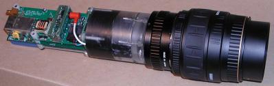
The Model 303 High Speed Gated Intensified Camera
My intention to increase camera frame rate was mentioned in the “TODO” section of the previous article, but the way to actually do that turned out to be very different from what I had anticipated. I decided not to use the JPEG-2000 compressor chip from Analog Devices. Nor did I make use of the new ETRAX multi-chip module from Axis Communications, as I wanted more memory (both SDRAM and Flash) than Axis put into the MCM version of its ETRAX controller. Also, in the new camera there was no place for a Quicklogic FPGA that I had intended to use for fixed-pattern noise elimination; this function needs 10 times less resources than image compression, and definitely fits in the same FPGA.
Instead, what I began to contemplate was . . .
An Open Source reconfigurable camera
I first investigated the possibility of using a large enough reprogrammable FPGA to be able to handle basic image acquisition tasks, fixed-pattern noise elimination, and image compression (i.e. baseline JPEG), without slowing down a sensor (~20 MHz pixel rate). An additional goal was to be able to use free FPGA development software, so it would make sense for me to post Verilog sources so that users would be able not only to build the camera software from sources but to do the same with the hardware (FPGA) part.
Incidentally, I'm not sure if it still makes sense to call it “hardware”, as you do not even need to open the case to modify it. But there are at least two arguments that it still is hardware: (1) it's easy to fry the thing, by installing the wrong code in the FPGA (I had to hold my finger on the chip while first debugging the download process); and (2) the speed — namely, a nearly 100x increase in compression performance and the fact that my Athlon-700 based PC is about 2.5 times slower in decoding than the camera FPGA in encoding (both require approximately the same amount of calculations) and the FPGA does not have any heat sink and is just slightly warmer than the environment.
Picking an FPGA
It was not difficult to find a good FPGA candidate. The latest member of Xilinx's low-cost Spartan IIe FPGA family — a 300K gates XC2S300E chip (see note below, for an update). Plus, they have free ISE Webpack development software available for download that worked fine for the design and was able to make use of 98% of the chip's resources.
Unfortunately, the free version of the 3rd party simulator Xilinx included with their free development software package proved useless for my purposes, as its 500 line limit is not serious for simulating such a design. I do not think this is a real problem for the Linux community, since some of the Open Source simulators can probably be combined with the Xilinx ISE for Linux.
Before starting an actual design, I had to evaluate whether the JPEG compressor and other required circuitry would fit into the selected FPGA (I did not have prior experience with Xilinx devices). So I looked for commercial IPs and found that they really do exist (although they're rather expensive), and thereby determined that the chip should handle the job.
I also located an XAPP610 application note which includes source code for an 8×8 DCT core that is fast enough and uses less than 30% of the chip (I later found out that I had to modify it).
Architecture of the Model 313
I didn't get around to really starting the new design until August, at which time I downloaded the Xilinx development software and designed the schematic and PCB layout for the Model 313 camera, making it exactly the same physical dimensions as the old one.
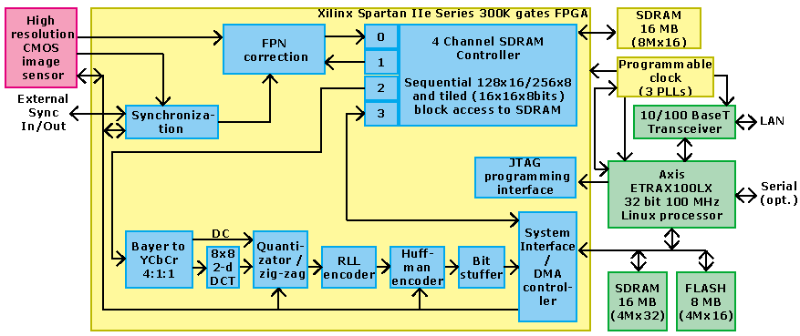
Block diagram: Model 313 Reconfigurable Network Camera
(click to enlarge)
Together with the new FPGA came some other components . . .
- 16MB SDRAM memory, connected directly to the FPGA so image processing does not reduce CPU bus bandwidth.
- multi-channel programmable clock: its 20 MHz crystal oscillator output and one of the three PLLs (25MHz) are used to drive ETRAX100LX and Ethernet transceiver respectively, leaving the two other PLLs for FPGA flexible clocking. This Cypress CY22393FC part combines EEPROM memory (so the right frequencies will be applied to the CPU and network transceiver upon power up) and the I2C-compatible interface making it possible to provide an extra degree of flexibility to a reconfigurable FPGA.
The SRAM-based FPGA is configured using the bit-stream file that is generated by the Xilinx development software and stored in the camera flash memory. It is transferred to the chip using just 4 pins of the ETRAX general purpose interface port which is connected to the dedicated JTAG pins of the XC2S300E. It takes just a single line in one of the init scripts (“cat /etc/x313.bit > /dev/fpgaconfjtag”) and a fraction of a second to bring it to life.
The FPGA code is designed around a four channel SDRAM controller. It uses internal “Block RAM” embedded memory (there are 16 of 4096 bit blocks in the XC2S300E chip) for ping-pong buffering of each channel. The controller provides interleaved access to the following channels . . .
- Channel 0 — raw or processed, 8 or 16 bits per pixel data from the sensor to the memory. Data is arranged in horizontal 256 pixel lines (128 for 16-bit data). It is also possible to write partial blocks (last in a scan line).
- Channel 1 — used to read from the memory per-pixel calibration data prepared by software in advance. For each pixel, there is an 8-bit value to subtract from the 10-bit sensor data. This data may be prescaled by 1, 2, or 4. The other byte contains sensitivity calibration, so depending on a global prescaling factor each pixel value may be individually adjusted in the +/- 12.5%, +/-25% or +/- 50% range.
- Channel 2 — provides data for the JPEG encoder. For the 4:2:0 encoding where two color components (Cb and Cr) have half of brightness resolution in both directions (that matches the Bayer color filters of the sensor) the minimal coding unit (MCU) is a square of 16×16 pixels that are later encoded as 4 8×8 blocks for the intensity (Y) component, and one 8×8 for each of Cb and Cr color ones (total 6 per MCU). If the data is encoded “live”, the SDRAM controller provides a “ready” signal for this channel whenever there are at least 16 lines written by the sensor (channel 0).
- Channel 3 — provides CPU access to the SDRAM. Normally it is used to read out raw sensor data and write calibration data for the FPN elimination (that is calculated by the CPU from the raw pixel data).
The SDRAM controller runs at 75MHz (16-bit wide data), which is enough for a pixel rate of up to 25MHz and quasi-simultaneous channel operation.
The synchronization module provides the camera with the capability of registering short asynchronous events. The camera is designed to work with both Zoran (2/3, 1/2, and 1/3 in.) and Kodak (1/2 in.) imagers which can work only in continuous “rolling shutter” mode. In that case, an asynchronous event (i.e. a laser pulse) will likely be registered in two consecutive frames (part in the first, and the balance in the second), but since the camera is continuously writing data into a circular buffer it is possible to reconstruct the complete image. The synchronization module can work in 2 ways: using an external electrical signal, or just comparing average the pixel value in each scan line with some predefined threshold. This makes it possible to register short light pulses without any additional electrical connections to the camera.
The JPEG compression itself is performed in a chain of stages, some of them using embedded Block RAMs as buffers and/or data tables (quantization and Huffman). This function uses approximately two-thirds of the resources of the FPGA . . .
- First stage — the Bayer-to-YCbCr converter receives 16×16 pixel MCU tiles and writes simultaneously into two buffers: one, 16×16 for Y data; and the other, 2x8x8 for Cb and Cr data. In parallel, it calculates average pixel value (DC component) for each of them and subtracts it on the output to bypass the DCT conversion. On the output, data goes out from the buffers in 64-sample (9 bits signed) blocks, 4 for Y component followed by 1 Cb an 1 Cr. The next 3 stages (DCT, Quantizator/Zigzag reorderer, and RLL encoder) are designed to process data in blocks of 64 consecutive samples with arbitrary (>=0) gaps between them.
- Second stage — the 8×8 DCT converter is based on a Xilinx reference design described here (PDF download). I had to modify it to make it work in asynchronous mode, so each 64-sample block can start with arbitrary delay (0 or more cycles) after the previous one, and to increase the dynamic range (the test fixture in the reference design had just 6-bit — not 8-bit — input data). This stage uses a 2x64x10-bit ping-pong memory buffer between horizontal and vertical stages of the 2-d DCT. Output data comes in the down first, then right order for each 64-sample block.
- Third stage — the Quantizator/Zigzag reorderer receives 8-bit signed average block value (directly from Bayer-to-YCbCr converter stage) and combines it with 12 bit signed data output from the DCT. It uses Two Block RAMs – one to store 2 alternative 2-table sets of 64×12-bit quantization data, the other – to reorder the output data in zigzag order (starting from the lowest frequencies and going to the highest) as required by the JPEG standard. This reordering increases the probability of long sequences of zeroes that are encoded on the next RLL stage. Quantizator uses uses multiplication by 12 bits (together with >>12) instead of division by 8 bits. The software that generates the tables makes corrections to the divisor table (written in the JPEG file header) so that for high divisor values they match the FPGA multiplicands). Quantization tables are written by the CPU prior to compression.
- Fourth stage — the RLL encoder is the first to break uniform 64-cycle long data packets. It combines the data output from the quantizator with the number of preceding zero-value data samples. This stage also maintains the previous DC value for each component (Y, Cb and Cr) and sends out the difference from the previous instead of the value itself for DC components.
- Fifth stage — the Huffman encoder uses 256x16bit FIFO for the input data it receives from RLL stage. Three more Block RAM modules (2x256x20) are required to store 2 sets of Huffman tables (one for Y, and the other – for Cb and Cr components). In each output 20-bit word 4 MSBs specify the number of bits to send, and the 16 LSBs – the data bits to send. The DC Huffman tables are rather short so they are stored in unused parts of the AC tables.
- Sixth stage — the bit stuffer receives number of bits to send and the data to send, combines them into continuous bit stream and formats into 16-bit output words. It also inserts 0x00 bytes after each 0xff, as the 0xff is a prefix to the marker in the JFIF data stream.
The output encoded data goes to a 256×16 FIFO and then is transferred to the system memory using CPU DMA channel as 32-bit long words.
Results and plans
The code compiles into 98% of the FPGA's resources. It takes about twenty minutes to compile on my 700 MHz Athlon PC. And it works — and works really fast! The compressor works at the full sensor rate (15 fps @1280×1024), and I can get 12 fps (some frames are still skipped) of the Quicktime format clips saved on the PC. There are a couple things that need to be cleaned up to fix that frame skipping, and then the camera will provide 15fps at 1280×1024 pixels, 60 fps at 640×480 pixels, and 240 fps at 320×240 pixels over the LAN connection.
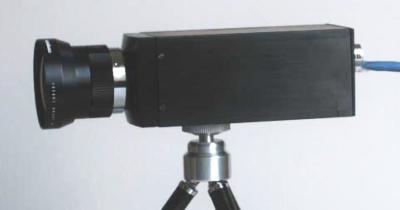
Model 313 Reconfigurable Network Camera
There is no video streaming server software in the camera yet. It can only provide Quicktime clips of some predefined length (although it is possible to make that length really big). To view the clips live (before they are completely transferred) all the index information is provided before the actual video data, so each JPEG frame is padded to make them all the same size. To make the size of the padding smaller (and make most of the frames fit) the JPEG compression quality is adjusted after each frame.
Incidentally, on November 18, 2002, Xilinx announced availability of two new members of Spartan IIe series, with 600K and 400K gates. The 600K uses a bigger package, whereas the 400K gates version has the option of matching the pinout of the XC2S300E currently used in the model 313 camera, so it can be used in the camera without any schematic of PCB changes. Using this device, I believe it will be possible to implement the full frame MPEG encoder.
Here is a product description of the resulting camera . . .
About the Elphel Model 313 Reconfigurable Network Camera
There are many network cameras (cameras that can serve images/video without computer) on the market today. Some can provide high frame rate video, but limited to 705×480 pixels or less. There are even some high-resolution (megapixel) network cameras, but they usually need one second or longer to compress a full size image.
The Model 313 can do both. It is a 1.3 megapixel network camera and it can serve full size images really fast — at 15 frames per second. High resolution may be very useful for security applications: for example, a single camera with a wide angle lens placed in the corner can see the whole room with the same quality as a narrow angle NTSC camera placed on a pan/tilt platform; and it can see it all at the same time, without any need of scanning.
Full resolution high frame rate even makes it possible not to use “digital pan-and-tilt” (sending out just a subwindow of the whole frame), the usual way to overcome the slow operation of high resolution network cameras.
The Model 313 camera is powered by 48VDC through the LAN cable, compliant to the IEEE 802.3af standard. This voltage makes possible to use four times longer cables to the camera than when using 24VDC power, and 16 times longer than 12VDC. Such lower voltages (not IEEE 802.3af compliant) are still used in some powered-over-LAN cameras.
All of the camera's embedded software and FPGA bitstream are stored in the camera flash memory, which can be upgraded through the Internet. Unlike the very dangerous procedure of rewriting flash memory with BIOS in a PC (if it was a wrong file or the power went off during flashing, the motherboard will likely be wasted), the Model 313 camera uses an important feature of the Axis ETRAX100LX 32-bit CPU which has an internal bootloader from the LAN that does not depend on the current flash memory data, so it is always possible to start over again with camera software installation.
Another important feature for developers is that both the embedded software and FPGA hardware algorithms are open source. Four levels of customization of the camera are thereby possible . . .
- Modification of the user interface using web design tools — The camera has three file systems that makes it easy and safe to modify preinstalled web pages and be able to restore everything back if something went wrong.
- Applications written in C — It is possible to compile C code on a computer running Linux after installing software from the downloads page (and links from there). The executable file may be transferred to the camera using ftp to RAM disk or a flash memory file system (jffs). That user application may have CGI interface, and can respond to http requests from the web browser.
- Adding (or modifying) drivers to the camera operating system — This will require building the new OS kernel and there are two ways to try it on the camera: boot the camera from the LAN with the new kernel (it will not change anything in the camera flash memory, so just turning it off and back on will restore initial software); or flashing it instead of original one (in that case, after power cycling camera will always boot with the new system).
- FPGA modification that gives full control over the power of the reconfigurable computing in the camera — This level requires different tools: FPGA development software from Xilinx (free for download available), and the camera sources posted on Elphel's website.
 About the author: Andrey N. Filippov has a passion for applying modern technologies to embedded devices, especially in advanced imaging applications. He has over twenty years of experience in R&D, including high-speed high-resolution, mixed signal design, PDDs and FPGAs, and microprocessor-based embedded system hardware and software design, with a special focus on image acquisition methods for Laser Physics studies and computer automation of scientific experiments. Andrey holds a PhD in Physics from the Moscow Institute for Physics and Technology. This photo of the author was made using a Model 303 High Speed Gated Intensified Camera.
NOTE: A version of this article translated into Russian is available here.
This article was originally published on LinuxDevices.com and has been donated to the open source community by QuinStreet Inc. Please visit LinuxToday.com for up-to-date news and articles about Linux and open source.