Flash memory does incredible shrinking act
Feb 1, 2010 — by LinuxDevices Staff — from the LinuxDevices Archive — 2 viewsIntel and Micron announced they've begin sampling 25-nanometer NAND flash technology, which will enable mobile devices and SSD (solid-state disks) to pack significantly more memory. Manufactured by the joint venture IM Flash Technologies, the process involves “the smallest semiconductor lithography available in the industry,” according to the companies.
According to Intel and Micron, the first product of their 25nm process — involving lithography 1/3000th the size of a human hair — is an 8GB NAND measuring just 167 x 167mm. As the companies point out, the device is small enough to fit through the hole in the middle of a compact disc, yet packs more than ten times the data capacity of that CD.
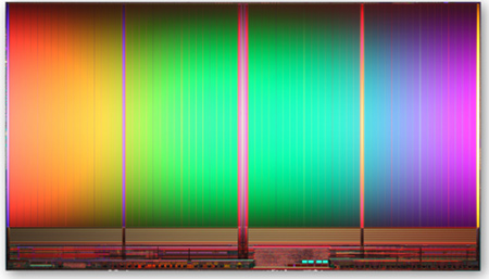
Intel and Micron say their 25nm NAND (shown much larger than life, below) is a single two-bits-per-cell multi-level-cell (MLC) die, capable of fitting into an industry-standard, thin small-outline package (TSOP). Reducing chip count by 50 percent compared to previous process generations, the 8GB device can be stacked in a package to increase storage capacity, the companies add.

The 25nm, 8GB NAND die from Intel and Micron
(Click to enlarge even further)
For example, it's said a 256GB SSD can now be enabled with 32 of these devices, versus 64 previously, a 32GB smartphone will require just four of them, and a 16GB flash card will require only two. As a result, the cost of flash memory is set to fall, while the amount of storage users can expect to see in mobile devices is set to increase, Intel and Micron say.
Intel and Micron formed IM Flash Technologies (IMFT) in 2006, and appear to have doubled NAND flash density roughly every 16 months. Production started with a 50nm process, eventually pushed to read speeds of up to 200MB/sec., and was followed by a 34nm process in 2008.
 Intel currently uses the 34nm parts in its popular 18-M and X25-MX SSDs (right), claimed to offer read latency of just 65 microseconds, along with five years of useful life (assuming 20GB of information being written to them per day). The 25nm parts will offer similar speed and longevity, Intel and Micron claim.
It's said the 25nm flash product uses Version 2.2 of the Open NAND Flash Interface (ONFI) specification, which currently permits the 200Mb/sec. transfer rate mentioned earlier in this story. IMFT is reportedly working on qualifying a future NAND flash product for ONFI's upcoming 3.0 specification, which has a data throughput rate of 400MB/sec.
Brian Shirley, VP of Micron's memory group, stated, "To lead the entire semiconductor industry with the most advanced process technology is a phenomenal feat for Intel and Micron, and we look forward to further pushing the scaling limits. This production technology will enable significant benefits to our customers through higher density media solutions."
Tom Rampone, Vp and GM of Intel's NAND solutions group, stated, "Through our continued investment in IMFT, we're delivering leadership technology and manufacturing that enable the most cost-effective and reliable NAND memory. This will help speed the adoption of solid-state drive solutions for computing."
Availability
According to Intel and Micron, their 25nm, 8GB NAND flash die is sampling now and is expected to enter mass production in the second quarter of this year. Meanwhile, Samsung announced last November that it, too, would slim down flash memory by moving to a 30nm process, though it did not say when the chips would go on sale.
This article was originally published on LinuxDevices.com and has been donated to the open source community by QuinStreet Inc. Please visit LinuxToday.com for up-to-date news and articles about Linux and open source.