Sony devices will talk to themselves wirelessly
Feb 8, 2010 — by LinuxDevices Staff — from the LinuxDevices Archive — 1 viewsSony announced a high-speed wireless technology designed for data transfer within electronic products. To be shown off this week at a conference in San Francisco, millimeter-wave transmission will increase reliability and decrease circuit board size, the company claims.
To date, most wireless technologies have been aimed at end users, and feature operational distances measured in feet, or at least inches. But according to Sony, its new "millimeter-wave" technology is designed to operate inside a device, over ranges of approximately two inches (50mm) at the most.
Why? Sony says the advancing functionality of today's electronics products requires ever-increasing quantities of internal data transfer in a device. As a result, the amount of wired circuitry required is leading to ever-more-complicated IC (integrated circuit) packages, intricately printed circuit boards, and larger IC sizes.
Therefore, claims the company, it makes sense to use wireless transmission as a means of communicating even inside a device. So doing will reduce the number of wired connections, minimize IC use, and simplify circuit boards, according to Sony. Since the data transfer occurs without contact, product reliability is also enhanced, especially when a device includes removable or detachable parts, the company adds.
According to Sony, its millimeter-wave technology employs electromagnetic waves with a frequency from 30GHz to 300GHz, and a wavelength between 1mm and 10mm. Because of their high frequency, such waves can transmit data at up to 11Gbps over short distances, the company notes.
Sony says it has used a 40nm production process to create a transmitter and receiver that, together, have a footprint of just 0.13 x 0.13mm. These components can be built into a single chip that consumes just 70mW, transmitting data over a distance of 0.55 inches (14mm) when a 0.03-inch (1mm) antenna is employed, the company adds. It's said that a larger, high-directivity antenna could extend range to about two inches (50mm).
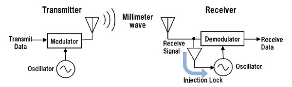
A block diagram of Sony's millimeter-wave intraconnect technology
English translation thanks to Engadget
(Click to enlarge)
The PLL (phase locked loop) circuitry traditionally used to align a receiver with the transmitted carrier frequency would have been too large and power-consuming for this application, according to Sony. However, the company claims, it has been able to adopt an "injection lock" system that eliminates PLL by injecting incoming signals into a receiver's oscillator, then aligning the oscillator to that signal.
Availability
Sony did not say when its millimeter-wave technology will be offered in commercial devices. However, a team of ten researchers from Sony Japan and one from the California Institute of Technology at Pasadena will give their presentation, "A Millimeter-wave Intraconnect Solution," at this week's International Solid-State Circuits Conference (ISSCC) in San Francisco.
More information on the presentation, which will be given at 1:30 PM on Wednesday, Feb. 10, may be found on the ISSCC website, here.
Sony's press release announcing its millimeter-wave technology may be found here. The Engadget item from which the translated block diagram above was taken can be found here.
This article was originally published on LinuxDevices.com and has been donated to the open source community by QuinStreet Inc. Please visit LinuxToday.com for up-to-date news and articles about Linux and open source.