Intel launches 3D-ready Sandy Bridge processors
Jan 3, 2011 — by LinuxDevices Staff — from the LinuxDevices Archive — 9 viewsApparently seeking mind share in advance of this week's Consumer Electronics Show (CES), Intel is launching its “Sandy Bridge” processors. The “second-generation Core products” — all said to permit gaming and 3D HD video — include 15 new mobile processors, 14 new desktop CPUs, and ten different chipsets to go with them.
Intel's Sandy Bridge processors have been an open secret ever since the chipmaker provided preliminary details at its Intel Developer Forum (IDF) last September, touting a new microarchitecture, a 256-bit instruction set known as AVX (advanced vector extensions), enhanced GPUs (graphics processing units), and dedicated silicon for tasks such as transcoding video from one format to another. Some of the model numbers for the Core-branded devices were subsequently leaked by Taiwanese sources.
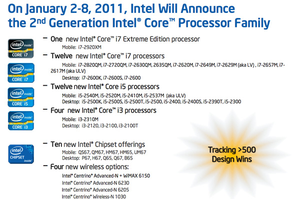
A summary of Intel's new Sandy Bridge products
Source: Intel
(Click to enlarge)
The company was originally expected to announce the Sandy Bridge devices on Jan. 5th, but is now making their release a week-long feast, as indicated by the above slide. Intel refers to the new CPUs as its "second generation Core processor family," which — as this lucid post by Daily Tech's Jason Mick points out — is confusing, not least because the company has already marketed processors using the "Core 2" brand.
Intel's original Core 2 CPUs ("Merom") debuted using a 65nm production process in 2006, and by 2008 were die-shrunk in the form of the 45nm "Penryn" versions. These CPUs were descendants of the P6 microarchitecture used by the Pentium Pro, Pentium II, Pentium III, and Pentium M, however, and did not feature the hyperthreading technology found in Pentium 4 CPUs.
In early 2009, therefore, Intel launched its new "Nehalem" architecture, billing it as the biggest breakthrough since the Pentium Pro. Initially found in server-oriented Xeon chips, Nehalem included not only hyperthreading but also TurboBoost technology, enabling one or more processor cores to run faster than the base operating frequency according to workload.
Nehalem moved to desktops and entry-level servers later in the year with the release of the Core i5, i7, and Xeon 3400 CPUs. The architecture then gained a 32nm die-shrink plus on-chip graphics via the January 2010 launch of "Westmere" processors, with Core i3, i5, and i7 branding.
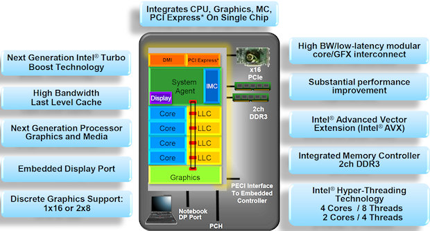
An overview of the new architecture on Intel's Sandy Bridge CPUs
Source: Intel (Click to enlarge)
Intel's Sandy Bridge chips (above) retain the 32nm production process, as well as the Core i3, i5, and i7 monikers, but gain an extra numeral in their names. The new processors are the chipmaker's first to put the CPU, memory controller, and GPU (graphics processing unit) all on one die, and provide all these components with a common L3 cache, ranging from 3MB to 8MB depending on model.
(Quips the Tech Report's Scott Wasson, "how [the Sandy Bridge chips] … are the second generation of anything with a Core name on it is beyond me.")
According to Intel, an enhanced version of TurboBoost technology now can vary the clock speed of the Sandy Bridge processors' GPUs as well as their CPUs, allowing the graphics cores to scale from 650MHz to 1.3GHz. All models are said to be capable of full HD video, even in 3D, and compatibility with a wide range of modern gaming titles is also touted.

New Sandy Bridge features
Source: Intel (Click to enlarge)
As was promised last year, the chips all support Intel's new AVX extension for increased floating point performance, as well as AES (Advanced Encryption Standard) instructions for hardware-based encryption. The new Quick Sync hardware video encode engine offloads video file conversion in hardware, the company adds.
End users or manufacturers wanting to incorporate Sandy Bridge CPUs in desktop devices will need to invest in new motherboards, since the processors incorporate a new Socket 1155 design, slightly different from the Socket 1156 used by Nehalem processors. And, though there's more functionality on board the processors than ever, Intel is also announcing ten new chipsets to accompany them: the QS67, QM67, HM67 (below left), HM65, and UM67 for mobile devices, and the P67 (below right), H67, Q65, Q67, and B65 for desktops.
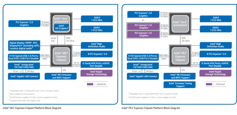
A block diagram of Intel's HM67 (left) and P67 (right)
Source: Intel (Click to enlarge)
Intel's naming scheme for the new Sandy Bridge offerings does little to help indicate how many cores a given device has, and it conveys only a vague idea of relative performance. On the desktop CPUs, a "K" tacked onto the name means an unclocked core multiplier, making overclocking possible. An "S" indicates a more energy-efficient offering, while a "T" indicates the greatest power savings possible for a given performance level.
| Model | Cores/threads | Clock speed/Turbo Boost | L3 Cache | Graphics speed/Turbo | TDP | Price (1Ku) |
| Core i7-2600K | 4 / 8 | 3.4 / 3.8GHz | 8MB | 850 / 1.350MHz | 95 W | $317 |
| Core i7-2600 | 4 / 8 | 3.4 / 3.8GHz | 8MB | 850 / 1.350MHz | 95 W | $294 |
| Core i7-2600S | 4 / 8 | 2.8 / 3.8GHz | 8MB | 850 / 1.100MHz | 65 W | n/a |
| Core i5-2500K | 4 / 4 | 3.3 / 3.7GHz | 6MB | 850 / 1.100MHz | 95 W | $216 |
| Core i5-2500 | 4 / 4 | 3.3 / 3.7GHz | 6MB | 850 / 1.100MHz | 95 W | $205 |
| Core i5-2500S | 4 / 4 | 2.7 / 3.7GHz | 6MB | 850 / 1.100MHz | 65 W | n/a |
| Core i5-2500T | 4 / 4 | 2.3 / 3.3GHz | 6MB | 650 / 1.250MHz | 45 W | n/a |
| Core i5-2400 | 4 / 4 | 3.1 / 3.4GHz | 6MB | 850 / 1.100MHz | 95 W | $184 |
| Core i5-2400S | 4 / 4 | 2.5 / 3.3GHz | 6MB | 850 / 1.100MHz | 65 W | n/a |
| Core i5-2390T | 2 / 4 | 2.7 / 3.5GHz | 3MB | 650 / 1.100MHz | 35 W | n/a |
| Core i5-2300 | 4/4 | 2.8/3.1GHz | 6MB | 850/1,100MHz | 95W | $177 |
| Core i3-2120 | 2 / 4 | 3.3 / – GHz | 3MB | 850 / 1.100MHz | 65 W | $138 |
| Core i3-2100 | 2 / 4 | 3.1 / – GHz | 3MB | 850 / 1.100MHz | 65 W | $117 |
| Core i3-2100T | 2 / 4 | 2.5 / – GHz | 3MB | 650 / 1.100MHz | 35 W | n/a |
"Sandy Bridge" desktop CPUs
Source: Intel
The mobile processors, meanwhile, have their own set of alphabetical suffixes, as explained by DailyTech's Mick:
The most common is M, which simply means (dual-core) mobile processors, and "QM" means quad-core mobile processors. "XM" means you have an unlocked multiplier. "LM" means a low-voltage mobile processor. And "E", "QE", and "LE" stand for an embedded (dual-core) mobile CPU, a quad-core embedded mobile CPU, and a low-voltage (dual-core) embedded mobile CPU, respectively.
| Model | Cores/ threads |
Base core clock speed |
Peak Turbo clock speed |
L3 cache size |
DDR3 speed | TDP | Price |
| Core i7-2920XM | 4/8 | 2.5 GHz | 3.5 GHz | 8 MB | 1600 MHz | 55W | $1096 |
| Core i7-2820QM | 4/8 | 2.3 GHz | 3.4 GHz | 8 MB | 1600 MHz | 45W | $568 |
| Core i7-2720QM | 4/8 | 2.2 GHz | 3.3 GHz | 6 MB | 1600 MHz | 45W | $378 |
| Core i7-2620M | 2/4 | 2.7 GHz | 3.4 GHz | 4 MB | 1333 MHz | 35W | $346 |
| Core i5-2540M | 2/4 | 2.6 GHz | 3.3 GHz | 3 MB | 1333 MHz | 35W | $266 |
| Core i5-2520M | 2/4 | 2.5 GHz | 3.2 GHz | 3 MB | 1333 MHz | 35W | $225 |
Standard-voltage mobile offerings
Source: The Tech Report
| Model | Cores/ threads |
Base core clock speed |
Peak Turbo clock speed |
L3 cache size |
DDR3 speed | TDP | Price |
| Core i7-2635QM | 4/8 | 2.0 GHz | 2.9 GHz | 6 MB | 1333 MHz | 45W | N/A |
| Core i7-2630QM | 4/8 | 2.0 GHz | 2.9 GHz | 6 MB | 1333 MHz | 45W | N/A |
| Core i5-2410M | 2/4 | 2.3 GHz | 2.9 GHz | 3 MB | 1333 MHz | 35W | N/A |
| Core i3-2310M | 2/4 | 2.1 GHz | N/A | 3 MB | 1333 MHz | 35W | N/A |
"Transational" (non-retail) mobile offerings
Source: The Tech Report
| Model | Cores/ threads |
Base core clock speed |
Peak Turbo clock speed |
L3 cache size |
DDR3 speed | TDP | Price |
| Core i7-2649M | 2/4 | 2.3 GHz | 3.2 GHz | 4 MB | 1333 MHz | 25W | $346 |
| Core i7-2629M | 2/4 | 2.1 GHz | 3.0 GHz | 4 MB | 1333 MHz | 25W | $311 |
| Core i7-2657M | 2/4 | 1.6 GHz | 2.7 GHz | 4 MB | 1333 MHz | 17W | $317 |
| Core i7-2617M | 2/4 | 1.5 GHz | 2.6 GHz | 4 MB | 1333 MHz | 17W | $289 |
| Core i5-2537M | 2/4 | 1.4 GHz | 2.3 GHz | 3 MB | 1333 MHz | 17W | $250 |
Low-voltage mobile offerings
Source: The Tech Report
Availability
At the time of writing, Intel had neither posted details of the new Sandy Bridge processors on its website nor announced availability details, as far as we were able to determine. According to a variety of sources, however, quad-core desktop models will be available this month, while others will go on sale during February.
This article was originally published on LinuxDevices.com and has been donated to the open source community by QuinStreet Inc. Please visit LinuxToday.com for up-to-date news and articles about Linux and open source.