Die-shrunk Cortex-A9 touted as 40 percent faster
Feb 16, 2010 — by LinuxDevices Staff — from the LinuxDevices Archive — 2 viewsARM Holdings and Globalfoundries have released new details of their upcoming, 28-nanometer HKMG (high-k metal gate) version of the Cortex-A9 processor. Entering production during the second half of this year, the device will improve performance by 40 percent, slash power consumption by 30 percent, and double standby battery life, the companies announced.
Last October, AMD and Globalfoundries announced a strategic relationship, described as a "broad agreement on processor implementation and circuit optimization to provide mutual customers with a robust enablement program." The agreement was to include a "full suite" of ARM physical IP, fabric IP, and processor IP, combined with Globalfoundries' HKMG manufacturing capabilities, according to the companies.
The companies said at the time that the first fruit of their alliance would be a 28nm implementation of ARM's high-end Cortex-A9 core (see later in this story for background). But, while HKMG's capability to provide "high-performance processing with minimal leakage" was touted, no claims were made about performance or power consumption.
These specifics have now been provided, thanks to an announcement yesterday at the Mobile World Congress (MWC) in Barcelona. Compared to 45nm or 40nm Cortex-A9 implementations, the die-shrunk 28nm versions will "provide approximately 40 percent higher performance within the same thermal envelope, delivering improved application performance and enriched multitasking capabilities on mobile devices," the companies stated.
It's said the 28nm parts will also provide a 30 percent reduction in power consumption, and a 100 percent increase in standby battery life. Production of the SoCs (system on chips) will begin during the second half of this year at Globalfoundries' Fab 1 in Dresden, Germany, the companies added.
ARM president Tudor Brown stated, "The transition to the 28nm technology node will be an important inflection point for wireless technology. Our collaboration with Globalfoundries will enable customers to rapidly bring high-performance, low-power ARM technology-based designs to market on a 28nm HKMG technology that is ready for high-volume implementation."
The ever-shrinking Cortex-A9
Announced in Oct. 2007, ARM's Cortex-A9 core was promoted from the outset as supporting clock speeds over 1GHz and performance of around 2,000 Dhrystone MIPS. The A9 also arrived with support for ARM'S MPCore interconnect technology, pictured below in a quad-core implementation.
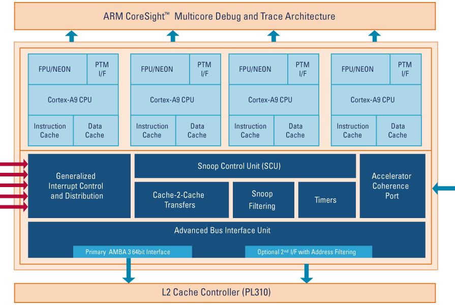
ARM Cortex A9 in MPCore configuration
(Click to enlarge)
Originally envisioned as being manufactured on TSMC's 65nm process, the Cortex-A9 has been steadily shrinking, reaping potential savings in both board real estate and power consumption. A year ago, for instance, ARM licensee Texas Instruments (TI) announced a 45nm, dual-core Cortex-A9 implementation, the OMAP4430 and OMAP4440, including Imagination Technologies' PowerVR SGX540 graphics and claimed 1080p video encode/decode. (The OMAP4 SoCs are sampling now and will enter production during the second half of this year, TI said yesterday.)
Last September, ARM announced 40nm Cortex-A9 implementations, code-named "Osprey," that can achieve clock speeds above 2GHz and are claimed to offer up to twice the performance of Intel's 1.6GHz Atom N270. Designed for TSMC's 40nm process, the dual-core Ospreys can run at 800MHz, consuming 0.5 Watts overall, or at 2GHz, consuming just 1.9 Watts, the company said.
Nvidia, too, announced a dual-core, 40nm Cortex-A9 implementation, the Tegra 250, in January. The SoC will provide "days" of battery life, dual-display support, bumps maximum resolution up to 1920 x 1080 pixels via HDMI or 1600 x 1050 on an LCD, and has HD encode as well as decode, the company says.
Earlier this month, NEC announced its Cortex-A9-based EMMA Mobile/EV1 and Mobile/EV2 SoCs (production process unstated, but most likely 45nm). The EV1 includes a single core, while the EV2 includes dual cores and the PowerVR SGX430 graphics engine, NEC says.
Background
AMD spun off Globalfoundries last year in a joint venture with ATIC (Advanced Technology Investment Company) of Abu Dhabi, and, until recently, has been the fab company's only customer. In July, Globalfoundries — which operates a manufacturing facility in Dresden, Germany, and is building another in upstate New York — gained STMicroelectronics as a client. (Globalfoundries is also in the process of buying Chartered Semiconductor, another foundry that numbers Broadcom and Qualcomm among its customers.)
For its part, ARM Holdings recently announced that more than 1.3 billion chips based on its designs were sold during the fourth quarter of last year. Shipments of Cortex-based chips more than doubled sequentially, though they were still only two percent of total shipments, the company added.
Availability
As noted earlier in this story, Globalfoundries and ARM say 28nm implementations of the Cortex-A9 will begin shipping during the second half of this year. Mobile World Congress attendees can view samples at the Globalfoundries booth (Hall 1, Stand 1F14) or the ARM booth (Hall 1, Stand 1C01), according to the companies.
General information on the Cortex-A9 may be found on the ARM website, here.
This article was originally published on LinuxDevices.com and has been donated to the open source community by QuinStreet Inc. Please visit LinuxToday.com for up-to-date news and articles about Linux and open source.