ARM Cortex-A9 processors get smaller, as 2.5GHz versions are tipped
Sep 2, 2010 — by LinuxDevices Staff — from the LinuxDevices Archive — 11 viewsGlobalfoundries says it has reached a “significant milestone” in its production of 28-nanometer ARM Cortex-A9 processors, with silicon expected in late 2010. While initial clock speeds could reach an Intel Atom-beating 2.5GHz, the company said further performance boosts for 28nm are in the works, and also provided its first timeline for the introduction of 22nm and 20nm manufacturing.
Last October, AMD and Globalfoundries announced a strategic relationship, described as a "broad agreement on processor implementation and circuit optimization to provide mutual customers with a robust enablement program." The agreement was to include a "full suite" of ARM physical IP, fabric IP, and processor IP, combined with Globalfoundries' HKMG manufacturing capabilities, according to the companies.
The companies said at the time that the first fruit of their alliance would be a 28nm implementation of ARM's high-end Cortex-A9 core (see later in this story for background).
Providing more details at last February's Mobile World Congress, the partners added that compared to 45nm or 40nm Cortex-A9 implementations, the die-shrunk 28nm versions would "provide approximately 40 percent higher performance within the same thermal envelope, delivering improved application performance and enriched multitasking capabilities on mobile devices."
It's said the 28nm parts will also provide a 30 percent reduction in power consumption, and a 100 percent increase in standby battery life. Production of the SoCs (system on chips) will begin during the second half of this year at Globalfoundries' Fab 1 in Dresden, Germany, or so the companies claimed in February.
A significant milestone
Now, Globalfoundries says it has reached a "significant milestone" in the production of ARM Cortex-A9s, taping out what's known as a TQV (technology qualification vehicle). This is "designed to emulate a product-like system-on-chip (SoC) in every way," allowing for maximum frequency analysis and short turnaround time between design cycles, the company says.
According to Globalfoundries, its TQV design uses a "fully optimized" ARM Cortex-A9 physical IP suite, including a full range of standard cell libraries, high-speed cache memory macros for L1 and density-optimized memories in other areas. A complete range of DFT (design for testability) features is said to enable "Silicon-Spice correlation" of Cortex-A9 critical paths and bit-mapping of cache memories at gigahertz speed.
"Silicon results are expected back from the fab in late 2010," the company adds.
Globalfoundries says the TQV is based on its 28nm HP (high performance) technology "for wired and high-performnance mobile applications," but the collaboration with ARM will also extend to an SLP (super low power) version "for power-sensitive mobile and consumer applications." In addition, the company announced, it will create ARM cores using a new, performance-enhanced HPP (high performance plus) technology.
The 28nm HPP technology will provide a ten percent performance boost over HP, as well as offering optional ultra-low leakage transistors and SRAMs that extend the application range from high performance into the low power range, Globalfoundries says. Scheduled "to begin risk production" during the fourth quarter of 2011, HPP will "address the growing market for smart mobile devices and high-performance processors requiring more than 2GHz of processing power," the company adds.
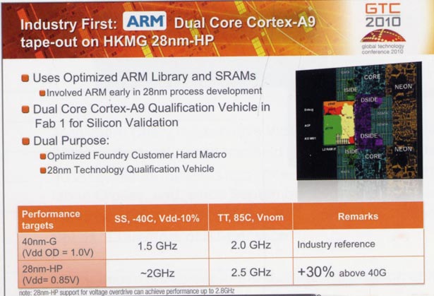
Globalfoundries' 28nm HP ARM Cortex-A9 implementation
Source: Bright Side of News
(Click to enlarge)
Though Globalfoundries' release did not further address clock speeds, a relevant slide (above) was reportedly displayed at the manufacturer's Global Technology Conference yesterday, then reproduced by the Bright Side of News website. The dual-core, 28nm Cortex-A9s will offer clock speeds ranging from 2.0GHz up to 2.5GHz, the slide appears to suggest.
A timeline for even smaller chips
Globalfoundries also provided its first timeline for the production of even smaller processors. The company's 22/20nm technologies will offer a "full node shrink" from 32/28nm, utilizing next-generation HKMG (high-K metal gate) technology and strain engineering "to enable the area and die cost scaling the industry has come to expect with each technology generation," the company says.
According to the manufacturer, "test chip shuttles" using 22/20nm technology will begin running in its Dresden, Germany-based Fab 1 in the second half of 2011. "Risk production" is set to begin in the second half of 2012, the company added.
It's said the 20nm technology offerings will come in HP and SLP varieties. The 22nm versions, meanwhile, will come in all three variants: HP, SLP, and HPP
Gregg Bartlett, Globalfoundries' senior vice president of technology and research and development, stated, "From the very beginning our vision has been to be the technology leader in the foundry industry. We ramped to volume production at the 45/40nm generation well ahead of all foundries and we are poised to maintain this leadership at 32/28nm, with plans to extend this to the 22/20nm node."
AMD spun off Globalfoundries in 2008 in a joint venture with ATIC (Advanced Technology Investment Company) of Abu Dhabi, and was for some time the fab company's only customer. In July 2009, Globalfoundries — which operates the above-mentioned fab in Germany and is building another in upstate New York — gained STMicroelectronics as a client. (Globalfoundries is also in the process of buying Chartered Semiconductor, another foundry that numbers Broadcom and Qualcomm among its customers.)
The ever-shrinking Cortex-A9
Announced in Oct. 2007, ARM's Cortex-A9 core was promoted from the outset as supporting clock speeds over 1GHz and performance of around 2,000 Dhrystone MIPS. The A9 also arrived with support for ARM's MPCore interconnect technology, pictured below in a quad-core implementation.
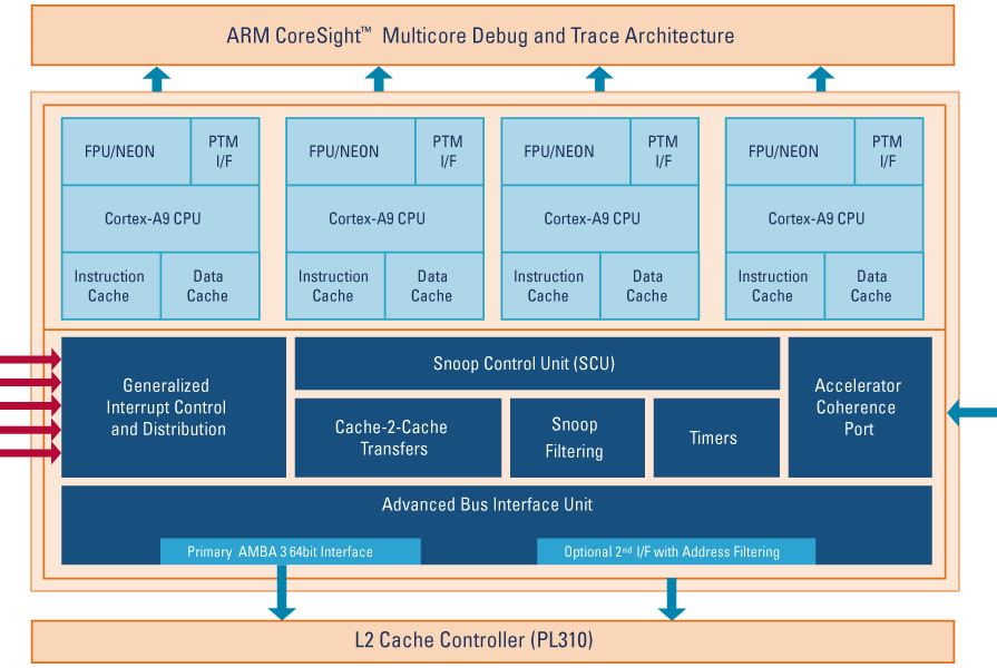
ARM Cortex A9 in MPCore configuration
(Click to enlarge)
Originally envisioned as being manufactured on TSMC's 65nm process, the Cortex-A9 has been steadily shrinking, reaping potential savings in both board real estate and power consumption.
A year ago, for instance, ARM licensee Texas Instruments (TI) announced a 45nm, dual-core Cortex-A9 implementation, the OMAP4430 and OMAP4440, including Imagination Technologies' PowerVR SGX540 graphics and claimed 1080p video encode/decode. (The OMAP4 SoCs are sampling now and will enter production later this year, TI said in February.)
Last September, ARM announced 40nm Cortex-A9 implementations, code-named "Osprey," that can achieve clock speeds above 2GHz and are claimed to offer up to twice the performance of Intel's 1.6GHz Atom N270. Designed for TSMC's 40nm process, the dual-core Ospreys can run at 800MHz, consuming 0.5 Watts overall, or at 2GHz, consuming just 1.9 Watts, the company said.
Nvidia, too, announced a dual-core, 40nm Cortex-A9 implementation, the Tegra 250, in January. Now shipping in a number of Android tablet computers, among other products, the SoC provides "days" of battery life, dual-display support, bumps maximum resolution up to 1920 x 1080 pixels via HDMI or 1600 x 1050 on an LCD, and has HD encode as well as decode, the company said.
Also earlier this year, NEC announced its Cortex-A9-based EMMA Mobile/EV1 and Mobile/EV2 SoCs (production process unstated, but most likely 45nm). The EV1 includes a single core, while the EV2 includes dual cores and the PowerVR SGX430 graphics engine, NEC said.
In July, meanwhile, STMicroelectronics (ST) announced an SoC (system on chip) claimed to be the industry's first to combine two ARM Cortex-A9 cores with a DDR3 memory interface. Currently sampling, the 55nm SPEAr1310 offers dual cores clocked at 600MHz, gigabit Ethernet, plus connectivity including USB, SATA, and PCI Express, the company says.
Further information
Background information on Globalfoundries' 28nm HKMG technology may be found on the company's website, here.
General information on the Cortex-A9 may be found on the ARM website, here.
This article was originally published on LinuxDevices.com and has been donated to the open source community by QuinStreet Inc. Please visit LinuxToday.com for up-to-date news and articles about Linux and open source.