Cortex-A9 SoC includes an FPGA, too
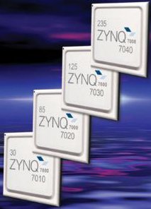
Mar 1, 2011 — by Eric Brown — from the LinuxDevices Archive — 11 viewsXilinx announced its first application processors in the form of Linux-ready, dual-core Cortex-A9 system-on-chip (SoCs) that offer FPGA functionality. The Zynq-7000 devices integrate dual 800MHz ARM Cortex-A9 cores with 28nm-fabricated, low-power programmable logic derived from the Xilinx Artix7 (Zynq-7010 and Zynq-7020) and higher-end Kintex-7 (Zynq-7030 and Zynq-7040) FPGA technologies.
The Zynq-7000 line of SoCs is billed as the industry's first Extensible Processing Platform (EPP), targeting high-end markets such as video surveillance, automotive driver assistance, and factory automation, among others. Xilinx announced its plans for EPP architecture SoCs last May, following an initial partnership agreement with ARM in Oct. 2009.
 As promised, the processor appears to be the first tight integration of ARM Cortex and FPGA (field programmable gate array) technology, a segment dominated by Xilinx. The FPGA technology incorporated in the Zynq chips offer "massive parallel processing to handle large amounts of data across a wide range of signal processing applications," says Xilinx.
PowerPC-based processors are used in FPGA products such as the company's Virtex-II Pro, Virtex-4 FX, and Virtex-5 FXT, along with IBM's Core Connect bus. However, the Zynq-7000 is the first FPGA/application processor hybrid that boots at power-up and can run a variety of operating systems independent of the programmable logic, says Xilinx. The processing system then configures the programmable logic on an as needed basis. What's more, the software programming model is "exactly the same as standard, fully featured ARM processor-based SoCs," says the company.
Although Xilinx said in October that it would continue to support PowerPC processors in other products, it appears that ARM represents the future for Xilinx. If nothing else, moving to ARM — and specifically to the powerful, dual-core Cortex-A9 architecture — should interest a whole new cross-section of embedded ARM customers.
The Zynq-7000 SoCs incorporate ARM dual-core Cortex-A9 cores with MPCore technology and integrated Neon and double precision floating point engines. The SoCs also include 32KB/32KB L1 and 512KB L2 caches, plus 256KB memory on-chip. A variety of memory controllers including DDR3 and NAND flash are also provided (see spec list farther below).
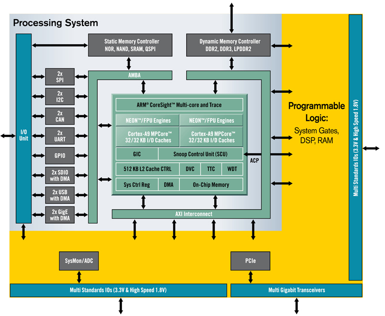
Zynq-7000 block diagram
(Click to enlarge)
Built on nine AXI interfaces, the interconnect is said to offer numerous control signals, representing more than 3000 interconnections. The interconnect enables designers to build their own custom devices by adding peripherals in the programmable logic. It is also touted as enabling designers to increase overall performance by partitioning hardware and software functions via custom accelerators.
The Zynq-7000 family's programmable logic is based on Xilinx's latest "7 series" FPGA architecture, thereby ensuring compatibility with earlier IP and tools "across all devices within the 28nm generation," says Xilinx.
The Zynq-7010 and Zynq-7020 devices are each based on the Artix-7 family, which is optimized for low-cost and low power, says the company. The larger Zynq-7030 and Zynq-7040 SoCs incorporate the more powerful Kintex-7 family of FPGAs and include between four and 12 10.3Gbps transceiver channels, as well as a PCI Express Gen2 block for high-speed off-chip connectivity.
All four devices are said to include a new dual 12-bit 1Msps ADC (Analog-to-Digital Converter) block. There was no mention of plans to extend the EPP architecture and Zynq-7000 line to incorporate the high end Virtex-7 technology.
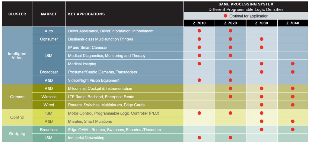
Application focus for each of the four Zynq-7000 SoCs
(Click to enlarge)
Features and specifications for the Zynq-7000 SoCs are said to include:
- Processor cores — 2 x ARM Cortex-A9 cores clock at up to 800MHz with Neon and single and double precision floating point units
- Cache — 32KB instruction and 32KB data L1; 512KB L2
- Memory:
- 256KB on-chip
- DDR2, DDR3, and LPDDR2 dynamic memory controllers
- QSPI, NAND flash, and NOR flash memory controllers
- I/O:
- 2 x gigabit Ethernet
- 2 x USB 2.0 (OTG)
- 2 x CAN 2.0 B
- 2 x SD/SDIO
- 2 x UART
- 2 x SPI
- 2 x I2C
- 32-bit GPIO
- Security — AES and SHA 256-bit encryption engine for secure boot and configuration
- ADC — Dual-channel 12-bit 1Msps analog-to-digital converter
- Interconnect — AMBA4 "Advanced Extensible Interface" (AXI4)
- Programmable logic features (general):
- 30k to 235k logic cells (approx. 560k to 4.7M of equivalent ASIC gates)
- 240KB to 1.86MB of extensible block RAM
- 80 to 760 18×25 DSP slices (58 to 912 GMACS peak DSP performance)
- Programmable logic features (by Zynq model):
- 7010 — 28K logic cells; 240KB block RAM; 80 DSP slices
- 7020 — 56k logic cells; 560KB block RAM; 220 DSP slices
- 7030 — 125k logic cells; 1060KB block RAM; 400 DSP slices
- 7040 — 235k logic cells; 1860KB block RAM; 760 DSP slices
- Programmable logic interfaces
- PCI Express Gen2x8 (in largest devices)
- 134 to 404 User I/Os (multiplexed + SelectIO)
- 4 x to 12 x 10.3Gbps transceivers (in largest devices)
Application developers can take advantage of both the Cortex-A9 and programmable logic capabilities via a portfolio of Xilinx and ARM design environments made available with the Zynq-7000 processors, says Xilinx. These are said to include:
- the Eclipse environment
- Xilinx Platform Studio Software Development Kit (SDK)
- ARM Development Studio 5 (DS-5)
- ARM RealView Development Suite (RVDS)
- Xilinx ISE Design Suite with AMBA4 AXI4 Plug-and-Play IP and Bus Functional Models (BFM)
The Zynq-7000 platform will also be supported by compilers, debuggers, and applications from the ARM Connected Community and Xilinx Alliance Program ecosystems, says Xilinx. These are said to include companies such as Lauterbach, Wind River, PetaLogix, The MathWorks, Mentor Graphics, Micrium, and MontaVista Software.
In the testimonials offered by the ecosystem partners, only PetaLogix and MontaVista specifically mention Linux support, but Wind River and Mentor Graphics are almost certain to support the chip with their respective Linux tools.
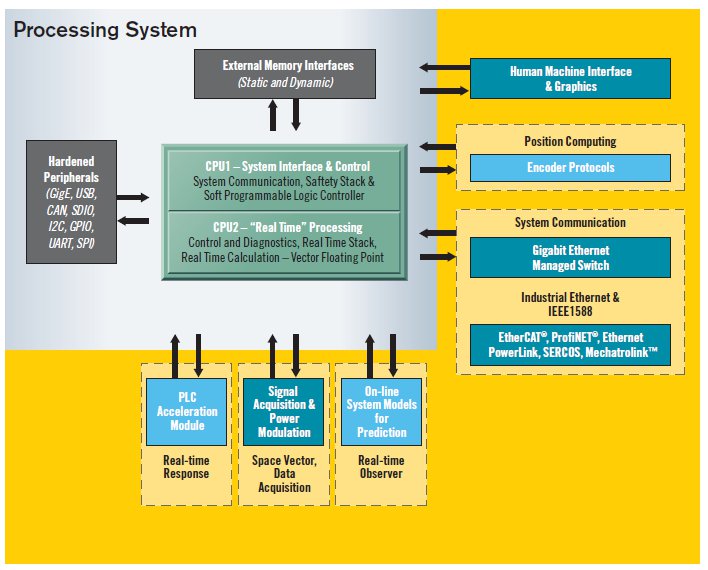
Typical industrial motor control application using Zynq-7000
(Click to enlarge)
Reference designs, development kits, and other resources from third parties, meanwhile, will target specific applications and design disciplines.
Stated Ralf Schaffer, project lead at Agilent Life Science Group, "For more than 10 years we have been discussing exactly this symbiosis possibility of processor and FPGA on one die to reduce cost and PCB space. Over time several companies have tried such an approach, but none of them offered a tight integration that allowed us to meet our targets. Finally, our long time wish becomes reality with the Xilinx Zynq-7000 family."
Stated Vin Ratford, Senior Vice President, Worldwide Marketing and Business Development at Xilinx, "The tight integration of the processing system with the programmable logic not only effectively reduces system bill of materials, power, and size, but will serve as an 'innovation engine' that can drive innovative applications and significantly expand the markets being served by traditional FPGA approaches to embedded systems."
Availability
First silicon devices based on the Zynq-7000 family are scheduled for the second half of 2011, with general engineering samples available in the first half of 2012, says Xilinx. Customers can start evaluating the Zynq-7000 family today by joining the Early Access program, which offers tools and development kits that support ARM to help designers familiarize themselves with the Cortex-A9 MPCore architecture and begin porting code. Pricing will start at below $15 in high volumes, but will vary and will depend on volume and choice of device.
More information may be found at the Xilinx Zynq-7000 page.
Xilinx is showing off the the Zynq-7000 Extensible Processing Platform family, including projects already under development, at Embedded World in Nuremberg, Germany, Mar. 1-3 at Hall 12/12-515.
This article was originally published on LinuxDevices.com and has been donated to the open source community by QuinStreet Inc. Please visit LinuxToday.com for up-to-date news and articles about Linux and open source.