Intel’s chipset recall will delay Sandy Bridge devices
Jan 31, 2011 — by LinuxDevices Staff — from the LinuxDevices Archive — 23 viewsIntel has announced a recall of the “Cougar Point” chipset designed to work with its “second generation” Core processors, warning that functionality of the devices' SATA ports could degrade over time. New versions of Cougar Point chipsets, such as the Q67 and QM67, are being manufactured now and will be delivered later this month, but “full volume recovery” isn't expected until April, the chipmaker says.
Intel's announcement of a flaw in its Cougar Point chipset temporarily takes some of the luster off the company's January launch of "Sandy Bridge" CPUs, the so-called second generation of its Core products. As we review later in this story, a pre-CES (Consumer Electronics Show) launch trumpeted 15 new mobile processors and 14 new desktop CPUs. Later on, six embedded-specific Sandy Bridge offerings came to light too via vendor announcements.

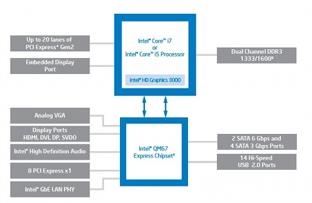
Intel's QM67 Express chipset
(Click to enlarge)
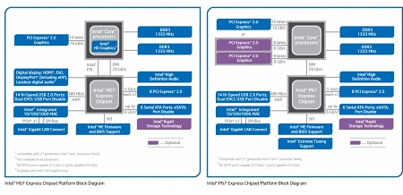
Since all the Sandy Bridge CPUs have on-chip graphics and memory controllers, they require only relatively simple I/O controllers, which are offered in at least ten models collectively code-named Cougar Point. The devices include the Q67, H67, H61, QM67 (above), HM67 (below left), P67 (below right), HM65, B65, and QS67.

Intel's HM67 Express chipset (left) and P67 Express chipset (right)
(Click to enlarge)
Intel's announcement early this morning highlights a "design issue" in the Cougar Point chips, for which it has had to implement a silicon fix. "In some cases, the SATA ports within the chipsets may degrade over time, potentially impacting the performance or functionality of SATA-linked devices such as hard disk drives and DVD-drives," the company says.
Intel adds that it is no longer shipping the affected chips, and has already begun manufacturing a new version that resolves the issue. First customer shipments will take place later this month, but "full volume recovery" will not be until April, adds the chipmaker.
It's difficult to say how the glitch will affect the delivery of Sandy Bridge-equipped embedded devices, especially because Intel didn't say if all the Cougar Point offerings have been affected (its announcement merely specifies the "6 Series"). All such devices we've encountered to date have employed the QM67 Express illustrated earlier in our story.
Intel did say the only Sandy Bridge devices that could be potentially affected are quad-core Core i5 and i7 systems. As these have only been shipping since Jan. 9, few customers are likely to have been impacted, the chipmaker claims, adding that it will "work with its OEM partners to accept the return of the affected chipsets, and plans to support modifications or replacements needed on motherboards or systems."
As Intel discontinues production of the current version of the chipset and begins manufacturing the new version, revenue for the first quarter of 2011 will be reduced by approximately $300 million, the company says. Total cost to repair and replace affected materials and systems in the market is estimated to be $700 million, the chipmaker added.
Separately, Intel recently announced that it had completed the acquisition of the Infineon Technologies AG Wireless Solutions business, which will now operate as the Intel Mobile Communications group. The company also expects to complete the acquisition of McAfee by the end of the first quarter.
The effects of the chipset issue and these transactions are incorporated into the company's revised outlook. Intel says it now expects first-quarter revenue to be $11.7 billion, plus or minus $400 million, compared to the previous expectation of $11.5 billion, plus or minus $400 million. Gross margin percentage is now expected to be 61 percent, plus or minus a couple percentage points, compared to the previous expectation of 64 percent, plus or minus a couple percentage points.
Background on Sandy Bridge
Intel's Sandy Bridge processors were an open secret ever since the chipmaker provided preliminary details at its Intel Developer Forum (IDF) last September, touting a new microarchitecture, a 256-bit instruction set known as AVX (advanced vector extensions), enhanced GPUs (graphics processing units), and dedicated silicon for tasks such as transcoding video from one format to another. Some of the model numbers for the Core-branded devices were subsequently leaked by Taiwanese sources.

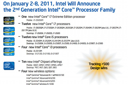
A summary of Intel's new Sandy Bridge products
Source: Intel
(Click to enlarge)
The company was originally expected to announce the Sandy Bridge devices on Jan. 5th, but wound up making their release a week-long feast, as indicated by the above slide. Intel refers to the new CPUs as its "second generation Core processor family," which — as this lucid post by Daily Tech's Jason Mick points out — is confusing, not least because the company has already marketed processors using the "Core 2" brand.
Intel's original Core 2 CPUs ("Merom") debuted using a 65nm production process in 2006, and by 2008 were die-shrunk in the form of the 45nm "Penryn" versions. These CPUs were descendants of the P6 microarchitecture used by the Pentium Pro, Pentium II, Pentium III, and Pentium M, however, and did not feature the hyperthreading technology found in Pentium 4 CPUs.
In early 2009, therefore, Intel launched its new "Nehalem" architecture, billing it as the biggest breakthrough since the Pentium Pro. Initially found in server-oriented Xeon chips, Nehalem included not only hyperthreading but also TurboBoost technology, enabling one or more processor cores to run faster than the base operating frequency according to workload.
Nehalem moved to desktops and entry-level servers later in the year with the release of the Core i5, i7, and Xeon 3400 CPUs. The architecture then gained a 32nm die-shrink plus on-chip graphics via the January 2010 launch of "Westmere" processors, with Core i3, i5, and i7 branding.

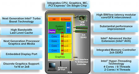
An overview of the new architecture on Intel's Sandy Bridge CPUs
Source: Intel (Click to enlarge)
Intel's Sandy Bridge chips (above) retain the 32nm production process, as well as the Core i3, i5, and i7 monikers, but gain an extra numeral in their names. The new processors are the chipmaker's first to put the CPU, memory controller, and GPU (graphics processing unit) all on one die, and provide all these components with a common L3 cache, ranging from 3MB to 8MB depending on model.
(Quips the Tech Report's Scott Wasson, "how [the Sandy Bridge chips] … are the second generation of anything with a Core name on it is beyond me.")
We complained last month that Intel's naming scheme for the new Sandy Bridge offerings does little to help indicate how many cores a given device has, and conveys only a vague idea of relative performance. On the desktop CPUs, a "K" tacked onto the name means an unclocked core multiplier, making overclocking possible. A "S" indicates a more energy-efficient offering, while a "T" indicates the greatest power savings possible for a given performance level.
The mobile processors, meanwhile, have their own set of alphabetical suffixes, as explained by DailyTech's Mick:
The most common is M, which simply means (dual-core) mobile processors, and "QM" means quad-core mobile processors. "XM" means you have an unlocked multiplier. "LM" means a low-voltage mobile processor. And "E", "QE", and "LE" stand for an embedded (dual-core) mobile CPU, a quad-core embedded mobile CPU, and a low-voltage (dual-core) embedded mobile CPU, respectively.
An exhaustive list of the 15 mobile and 14 desktop Sandy Bridge CPUs Intel announced in January may be found in our earlier coverage. Meanwhile, Intel never formally announced embedded versions (denoted by their "E" suffix), and still hasn't posted information about all of them on its website. Courtesy of vendor announcements, however, we've been able to piece together the list below.
| Processor | Cores /threads |
Base frequency (Ghz) |
1 core turbo (Ghz) | 2 core turbo (Ghz) | Last-level cache (MB) |
TDP (W) | ECC |
| Core i7-2710QE | 4/8 | 2.1 | 3.0 | 2.9 | 6 | 45 | no |
| Core i7-2715QE | 4/8 | 2.1 | 3.0 | 2.9 | 6 | 45 | yes |
| Core i7-2655LE | n/s | 2.2 | n/s | n/s | 4 | 25 | n/s |
| Core i7-2610UE | n/s | 1.5 | n/s | n/s | 4 | 17 | n/s |
| Core i5-2510E | 2/4 | 2.5 | 3.1 | 3.0 | 3 | 35 | no |
| Core i5-2515E | 2/4 | 2.5 | 3.1 | 3.0 | 3 | 35 | yes |
What we know about Intel's embedded-specific Sandy Bridge devices so far
As already noted, these embedded CPUs all use the QM67 Express chipset. This permits devices to offer up to fourteen USB 2.0 ports, two 6Gbps SATA ports, and four 4Gbps SATA ports, according to Intel.
Further information
More information about embedded devices that have already been launched wtih Intel's Sandy Bridge cores on board may be found via the links below.
This article was originally published on LinuxDevices.com and has been donated to the open source community by QuinStreet Inc. Please visit LinuxToday.com for up-to-date news and articles about Linux and open source.